Intel Celeron 500 MHz specifications
| General information |
| Type | CPU / Microprocessor |
| Market segment | Desktop |
| Family | Intel Celeron |
| CPU part number |
- FV80524RX500128 is an OEM/tray microprocessor
|
| Frequency ? | 500 MHz |
| Bus speed ? | 66 MHz |
| Clock multiplier ? | 7.5 |
| Package | 370-pin Plastic Staggered Pin Grid Array
1.95" x 1.95" (4.95 cm x 4.95 cm) |
| Socket | Socket 370 / PGA370 |
| S-spec numbers |
| Part number |
ES/QS processors |
Production processors |
|---|
| |
QD27 |
SL3FY |
| FV80524RX500128 | + | + |
|
| Architecture / Microarchitecture |
| Microarchitecture | P6 |
| Processor core ? | Mendocino |
| Core stepping ? | B0 (QD27, SL3FY) |
| CPUID | 665 (SL3FY) |
| Manufacturing process | 0.25 micron
19 million transistors |
| Data width | 32 bit |
| Floating Point Unit | Integrated |
| Level 1 cache size ? | 16 KB code
16 KB data |
| Level 2 cache size ? | 128 KB |
| Physical memory | 4 GB |
| Extensions and Technologies | |
| Low power features | - AutoHALT state ?
- Stop Grant state ?
- Sleep state ?
- Deep Sleep state ?
|
| Electrical / Thermal parameters |
| V core ? | 2V |
| Minimum/Maximum operating temperature ? | 5°C - 70°C |
| Maximum power dissipation ? | 27.2 Watt |
Detailed side-by-side comparison
FAQ
Q: Is it possible to upgrade my Celeron 500 MHz processor?
A: Probably yes. CPU compatibility is
determined by your motherboard. Please check CPU-Upgrade.com resource
for CPU support list for your board.
Celeron 500 MHz Overclocking
Sorry, we do not have overclocking data for this Intel Celeron processor at this time.
CPU ID information for the Celeron 500 MHz
Detailed characteristics of processor's internals, including x86
instruction set extensions and individual instructions, high- and low-level
technologies, are listed below. This list was acquired from an actual
Intel Celeron 500 processor with the help of the x86 CPUID instruction. Any
discrepancies between CPUID features and official specifications are
likely due to some features being disabled in BIOS, or due to a bug in
our CPUID decoding algorithm.
Different steppings of Intel processors may also have slightly different features.
Search or browse all public submissions in our CPUID database.
Use our CPU identification tool to check features of your processor.
| Submission details |
|---|
| Manufacturer: | Intel | Measured frequency: | 513 MHz |
| CPU Family: | Celeron | Comment: | |
| Processor Number: | 500 | |
| Part number (supplied): | FV80524RX500128 | Submitted by: | Neon |
| Part number (guessed): | FV80524RX500128 | Submitted on: | |
| S-Spec Number: | SL3FY | CWID version: | 0.3 |
General information
| Vendor: | GenuineIntel |
| Processor type: | Original OEM Processor |
| CPUID signature: | 665 |
| Family: | 6 (06h) |
| Model: | 6 (06h) |
| Stepping: | 5 (05h) |
| TLB/Cache details: | Data TLB: 4-KB Pages, 4-way set associative, 64 entries
Data TLB: 4-MB Pages, 4-way set associative, 8 entries
Instruction TLB: 4-KB Pages, 4-way set associative, 32 entries
Instruction TLB: 4-MB Pages, fully associative, 2 entries |
Cache details
| Cache: |
L1 data |
L1 instruction |
L2 |
|---|
| Size: |
16 KB |
16 KB |
128 KB |
| Associativity: |
4-way set
associative |
4-way set
associative |
4-way set
associative |
| Line size: |
32 bytes |
32 bytes |
32 bytes |
Supported instructions
| Instruction set extensions | Additional instructions |
|---|
| MMX |
CMOV |
| |
CMPXCHG8B |
| |
FXSAVE/FXRSTORE |
| |
SYSENTER/SYSEXIT |
Integrated features and technologies
| Major features | Other features |
|---|
| On-chip Floating Point Unit |
36-bit page-size extensions |
| |
Debugging extensions |
| |
Machine check architecture |
| |
Machine check exception |
| |
Memory-type range registers |
| |
Model-specific registers |
| |
Page attribute table |
| |
Page global extension |
| |
Page-size extensions (4MB pages) |
| |
Physical address extensions |
| |
Time stamp counter |
| |
Virtual 8086-mode enhancements |
CPUs, related to Intel Celeron FV80524RX500128 (500 MHz)
The list of related CPUs does not include all models. For the complete list, please see the related "P6" processors for socket 370 page.
• Within each category, the CPUs are sorted from slower (at the top) to faster (at the bottom)
• Background color of specs and features indicate whether they are better or worse than similar spec/feature of the Celeron FV80524RX500128 (500 MHz)
• Click on the
> icon to compare any CPU in the table with the Intel Celeron FV80524RX500128 (500 MHz) (Javascript required).
• Features abbreviations:
SSE - SSE instructions
Pictures (4)
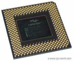
| Bottom view |
500 MHz
128 KB L2 cache
Plastic Pin Grid Array package (socket 370)
Bottom view |
 |
|
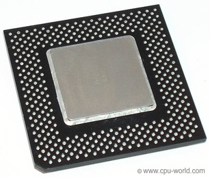
| Top view |
500 MHz
128 KB L2 cache
Plastic Pin Grid Array package (socket 370)
Top view |
 |
|
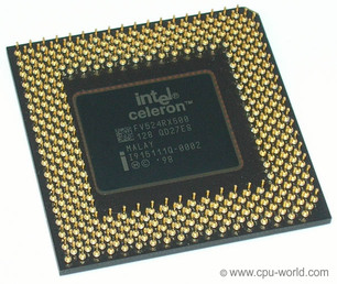
| Engineering sample - bottom view |
500 MHz
128 KB L2 cache
Plastic Pin Grid Array package (socket 370)
Engineering sample
Bottom view |
 |
|
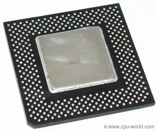
| Engineering sample - top view |
500 MHz
128 KB L2 cache
Plastic Pin Grid Array package (socket 370)
Engineering sample
Top view |
 |
|
|
Comments (1)
You're welcome to post suggestions, corrections, your own personal
Intel Celeron 500 MHz review, or your experience with the microprocessor.
Please do not ask upgrade and troubleshooting questions, and do not start
discussions.


Process size
The process size for these should be 250 nm.
I hate using Wikipedia to validate things, but under "List_of_Intel_Celeron_microprocessors", all Mendocino cores are reported as 250 nm.
Additionally, the SL3FY link on the page also confirms the 250 nm process size.